“Well-known manufacturers (they have a big name, for what I don’t understand)” from all over the world, they act as if they are gods, manipulating as they will, what they think that are a horde or herd of ignorant’s. They’re inventing unusable aberrant technologies, tools, devices (using pseudo-science, pseudo-technology) that electronics professionals are need for their own professional purpose.
After they invent their own aberrations, came the marketing team.
The marketing team act like a horde of predators, using the lowest possible social / moral / legal tools, that they have at their disposal, lies, cheating, disinformation and so on.
This combination between “well-known manufacturers” and that type of marketing, fore more than 40 years, was a recipe for success.
“Well-known manufacturers” all over the world, act as if they are gods, manipulating as they will, what they think that are a horde or herd of ignorant. They invent technologies, tools, devices that electronics professionals must use for their intended purpose.
ERSA review, the “well-known” ERSA manufacturer and their garbage, in general.
ERSA, as PDR-Rework… claim, quality, the word’s best ever approach, high yield, professional, expert, courses, world’s best support… you name it all that these thefts claim. ERSA claim all that with the only purpose that stole money from you. No proof about his affirmations. They are not alone… Finetech, Chinese manufacturers… All… are in…
1 – Worst practice ever. Along my professional life, I saw many aberrations. That aberration, to heat the PCB at 250 °C, I don’t see it until now.
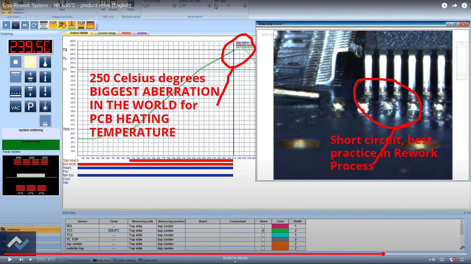
To heat the PCB / board at 250 °C is the worst ever practice that you can have. But… ERSA can’t measure the BGA / Chips temperature independent of PCB / Board temperature. In fact… measuring the PCB / board temperature with two temperature thermocouple (sensors say… ERSA), will be the second aberration that I’ll review. So… Exist Tg point. In general, Tg point is from 110 °C to 180 °C for FR-* types. ERSA claim / recommend that you need to heat the board above the highest (180 °C) Tg point. It claims / recommend / teach you that you heat the PCB / board at 250 °C. This is the worst practice ever.
More details about Tg point – worst practice – in general – click or touch or use menu to go.
Well… ERSA not only that recommend you to heat the PCB / board at 250 °C, but they affirm / claim that they have the best practice in the world. Using false / fake affirmations, pseudo-science, pseudo-technology, zero / 0 knowledge in electronic manufacturing, zero / 0 knowledge in practical electronic, zero / 0 knowledge in electronic service… They are zero / 0 pure and hard in… all… but give you advices, wrong advices.
More details about Temperature – PCB / board – worst practice – in general – click or touch or use menu to go.
So… Best practice / science / technology say, that you need to heat the PCB / board much lower than Tg point (Tg point from 110 °C to 180 °C). So… The temperature that you’ll heat the PCB / board MUST be under 100 °C. This is the best practice.
More details about Tg point – best practice – in general – click or touch or use menu to go.
Common sense. Your / mine experience in electronic say that you don’t heat the PCB / board every time when you change a resistivity, a capacitor, a I2C memory in SOT8, a flash memory, a microprocessor with 256 pins, when you do any of that you don’t heat the PCB / board at 250 °C. Overall, you won’t heat ever, never a PCB / board at 250 °C. This is best practice!
Why you don’t heat the PCB / board?! From science / technology / common sense point of view. You DO NOT want to have broken VIAS (VIAS – the little metalized with copper holes that connect electronically different layouts of the PCB / board). You don’t want to assume the RISK to have broken VIAS. Not only that, but you will want to protect your VIAS to avoid the appearing of the worst ever failure in electronics… The intermittent contact failure.
More details about Temperature – PCB / board – best practice – in general – click or touch or use menu to go.
2 – Worst ever practice. Not only use K-type thermocouple, mounted in a shield to elevate the thermocouple inertia, but… use 2 (two thermocouples)… On same PCB board. They think that with one measure, the BGA temperature… That it’s crazy. That amount of aberration, you need to see it… to believe it.
Let see… The K-type thermocouple (that almost sure that use ERSA in his garbage), are the worst ever world’s thermocouple (from accuracy point of view). In fact, the K-type thermocouple is used on device that need / work at high temperature (metal melting furnace, ceramic kilns… and so on) because this garbage K-type thermocouple withstand above or around 1200 °C. On this type of appliance, high accuracy is not important (± 15 °C are not important).
But on the Rework process profile standard, the same ignorant’s JEDEC / IPC, tell us that in the top of the rework profile that make the rework profile (let say… for the lead free profile… at 250 °C) you MUST be in 5 °C maximum errors. How a hell can you measure / have maximum 5 °C of error when your device / sensor with which measure that temperature has already 30 °C ??? Aberrations…
And ERSA not stop here, the aberration chain, use 2 / two K-type thermocouple to “measure” in two points the PCB temperature. Can’t count more… aberrations and… bullshit that that guy’s have in the place where the brain must be. I don’t speak about 0 / zero thermal contact between sensor and PCB / board. What a hell it measures here ERSA… only… pseudoscience and pseudo-technology from ERSA amputated brain… know.
K-type thermocouple – contact sensors – worst practice – in general – click or touch or use menu to go.
Close view to ERSA double aberration. That guy’s can. They can be so stupids. A real shame for electronics industry, for trues electronics professionals.
But… pay attention, please. They can heat a metallic top BGA, a little (about 30 mm square…) Xilinx in fact… Show the ERSA muscle in front of his competitor… PDR-Rework that can’t rework metallic top BGA without black tapes (the $70,000 tapes business…). But poor guys… only now they learn the fact that the only field where they fight are… aberrations, promiscuity, ignorance… and so on.
The K-type thermocouple MUST not be used on a real professional BGA Rework process or professional BGA Rework Stations. If is needed, and sometime is needed contact sensors, exist another types of contact sensors that have, for example, what I’ll use two models (NASA use same sensors) with ± 0.15 °C and 0.10 °C of maximum error. But wait… We need that accuracy on temperature measurement(± 0.15 °C or 0.10 °C)? If yes… why?!
Simple. If somebody says maximum 5 °C error for something, the tool that you’ll use to measure that temperature MUST be at last 10 times more accurate. That mean maximum error ± 0.5 °C. But that is for a step of 5 °C (0-5-10-15-20… and so on, this thing is named “resolution”). Well… 5 °C of resolution are not enough. You’ll need 1 °C resolution (1-2-3-4-5… and so on…) to express the 5 °C of error from the JEDEC / IPC standards. Well for that resolution, 1 °C, you’ll need 10 times less error accuracy. So… for that reason, we need about ± 0.1 °C.
And not forgot about NIST traceable certificate. It is not enough that PDR-Rework or ERSA or me say, we have ± 0.1 °C accuracy for temperature measurement… No sir, it’s not enough, that is only an affirmation… We need to prove that affirmation with… With A NIST traceable certificate. I can prove, but I don’t sell anything. ERSA, PDR-Rework and the rest… none can prove nothing more than… aberrations.
Contact sensors – best practice – in general – click or touch or use menu to go.
3 – Worst PCB heating temperature uniformity, must be nonuniform… As that ERSA… say / make. I think that ERSA invent something… How to screw up a PCB.
ERSA professional Rework pattern terror-error 1
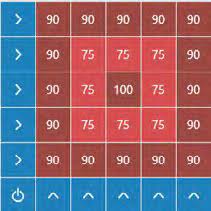
ERSA professional Rework pattern terror-error 2
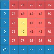
ERSA professional Rework pattern terror-error 3

Above we have three fine examples from ERSA release Terror-Error “professional Rework profiles”. The recipe for destruction. They forgot to take the pills!
ERSA present for you the new recipe for destruction. Before that… They forgot to take a visit at psychiatric doctor and over all they forgot to take the pills that same psychiatric doctor recommend them at a preview visit. That worst ever approach have a long time in the ERSA development. As already know, ERSA company are a German company buy his Chinese brothers. On the “ERSA” name, some Chinese people clean up a non-names and Germanize them.
But no-name ERSA can’t forget his roots. And as they saw that his Chinese brother have 3 heating zones on professional BGA Rework Stations (below, ex:)
As you see… The low-cost Chinese garbage can screw up on 3 / three zone a PCB / Board. Well… ERSA can do it better. ERSA can screw it up in all zones! Among that ERSA can destroy everything with ocean matrix wave… aberration!
PCB uniformity – the worst practice – in general – click or touch or use menu to go.
As from best practice approach point of view – You MUST heat and maintain the temperature of the PCB / board as uniform possible you can. In fact, I fight with the bottom heater in HRA (high resolution array) mode to achieve the best temperature uniformity that in practice is possible. Among high speed control (lowest possible inertia) and perfect non-contact multi zone temperature measurement.
PCB uniformity – best practice – in general – click or touch or use menu to go.
4 – Rework profile, how the ERSA “well-known manufacturer”, “revolutionize” the rework process graph in electronic industry. ERSA can’t respect anything.
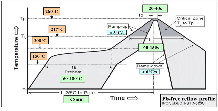
Original JEDEC / IPC reflow profile, that MUST respect.
Last aberrational revolution from ERSA
Old aberrational revolution from ERSA

As ERSA accustomed us, they invent. They invent aberrational, stupid, illogical and so on things. Here I’ll present you the Rework Process graph revolutions!
This guys from ERSA seems that have not only psychical problems but seems that his view it is severely affected. From any point of view, nor second or third image can fit somewhere how… in the first image. So ERSA continue his infinite chain of aberrational invention with only goal to destroy a PCB / board, to destroy a BGA / component. But they claim… Professionalism, best practice, expert and so on. Here I’ll never can stop to cont how worst they do that.
Rework profile – the worst practice – in general – click or touch or use menu to go.
In the first image, you’ll have the theoretical JEDEC / IPC (IPC the biggest scam in the world, I know that I say). The JEDEC /IPC REFLOW profile have at his base the common sense. It counts a combination of points that have a time and a temperature. After that, joining the points, resulting this beautiful graph. So far, so good. That graph has only some common sense point of view. For example, the oxidation removal flux / paste.
They pay attention, not only at oxidation removal flux / paste activation point, at oxidation removal flux / paste burning point. Also, the JEDEC / IPC pay a special attention to PCB / board stressing forces, at melting point of tin… In the original JEDEC / IPC, you’ll see that they pay a special attention at the time above liquid for the soldering alloy. The highest attention is taken for the highest temperature that the BGA Rework Station must fine / accurate control
Rework profile -best practice – in general – click or touch or use menu to go.
By the way… on the above image, you’ll have two thin red lines and two tin red circles. I’ll draw this lines and circles for some simple reasons.
When we look at something on internet (videos/ picture / text…) must know what we see, at what we look. ERSA post their aberration all over the internet. Almost all that look at the ERSA aberrations don’t know what they see. Let explain in short… what you see in above image. The lines that I’ll put overlaid on the image help you to see the lack of parallelism on the worst ever ERSA rework process. The two circles focus your attention on two different balls shapes.
As you see on above image, the BGA chip on the left side is close to PCB and in the bright side is less close to PCB. That mean that the BGA chip are oblique on the PCB. Left side close – right side less close. That mean that the balls from left side of BGA was soldered, and the balls from right side was in air / wasn’t soldered. A clear example about the worst ever approach, ERSA approach.
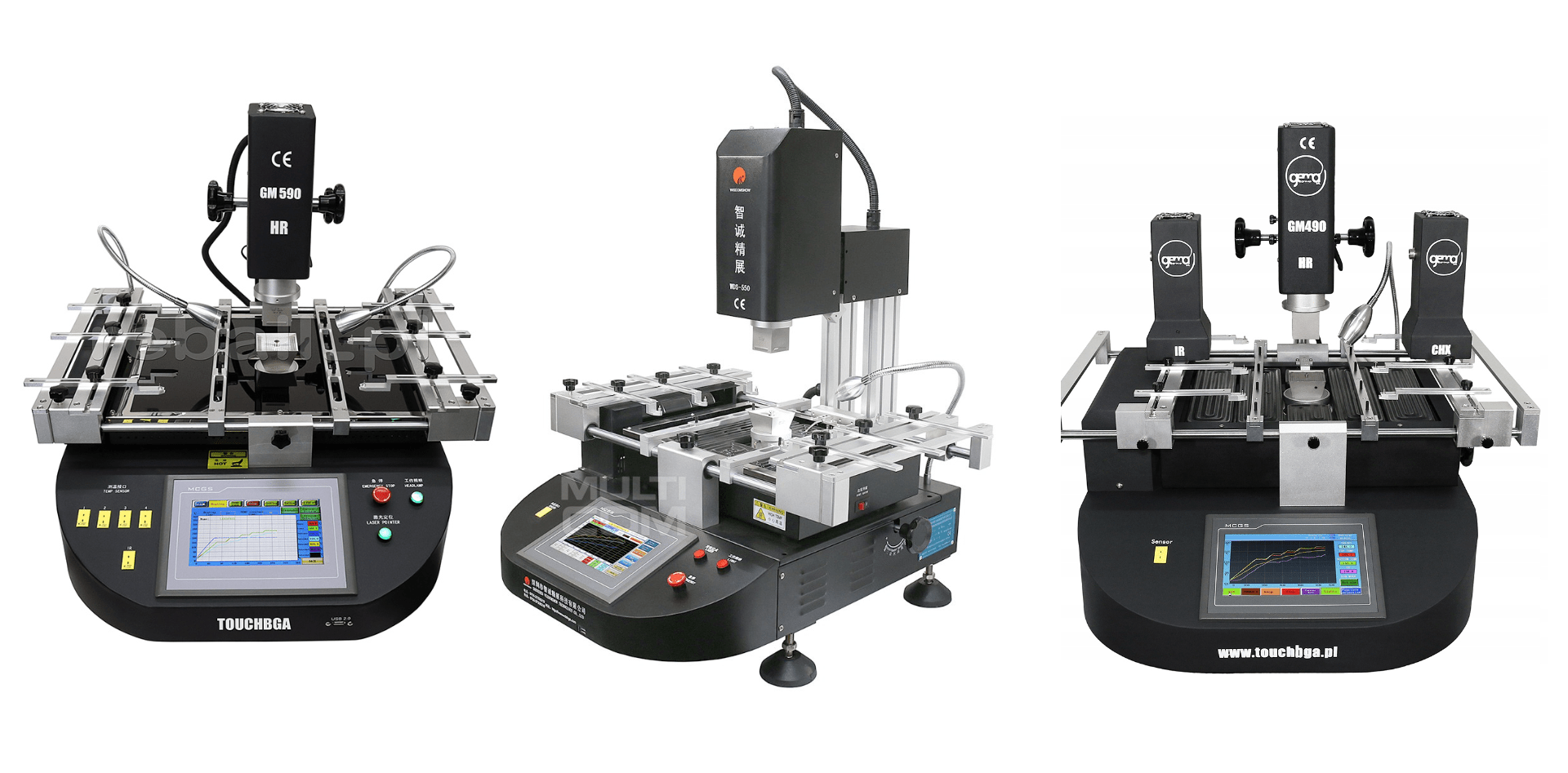
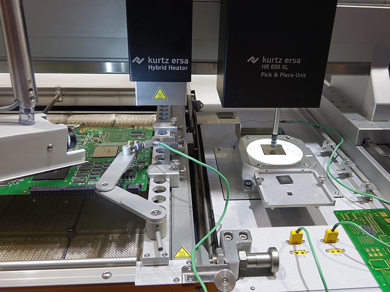
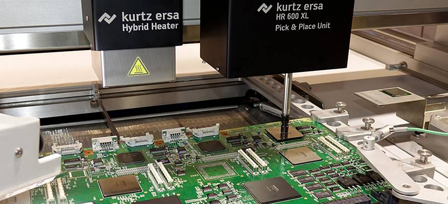
5 – Fixtures – another boring worst approach from ERSA aberrations chain. ERSA (like all others “well-known manufacturers”), Stuck the PCB / board.
To continue in his fight with the aberration / worst practice chain, ERSA stuck / fix / block the PCB / “big board aberration” in an aluminum frame. For ERSA that approach is “best approach”. Once more, ERSA demonstrate (if it was necessary) his lack in understanding electronics world, professional electronic world and so on. So… as how big is the PCB / board that is fixed by ERSA approach, on consequence path… the biggest aberrations are.
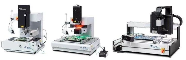
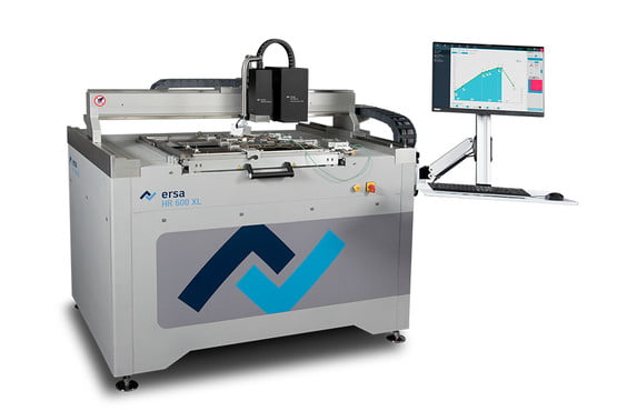
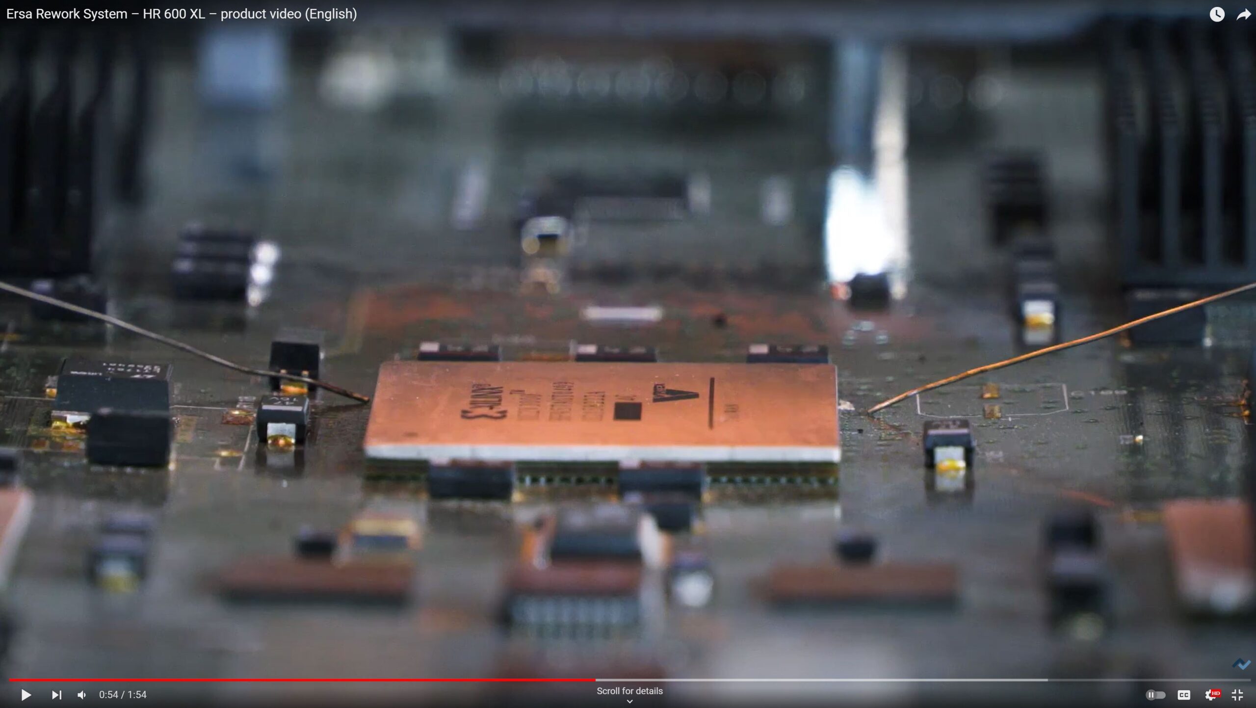
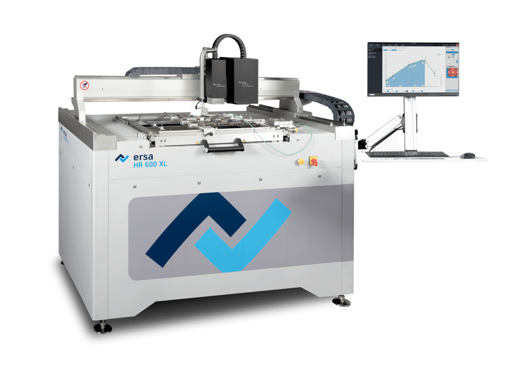
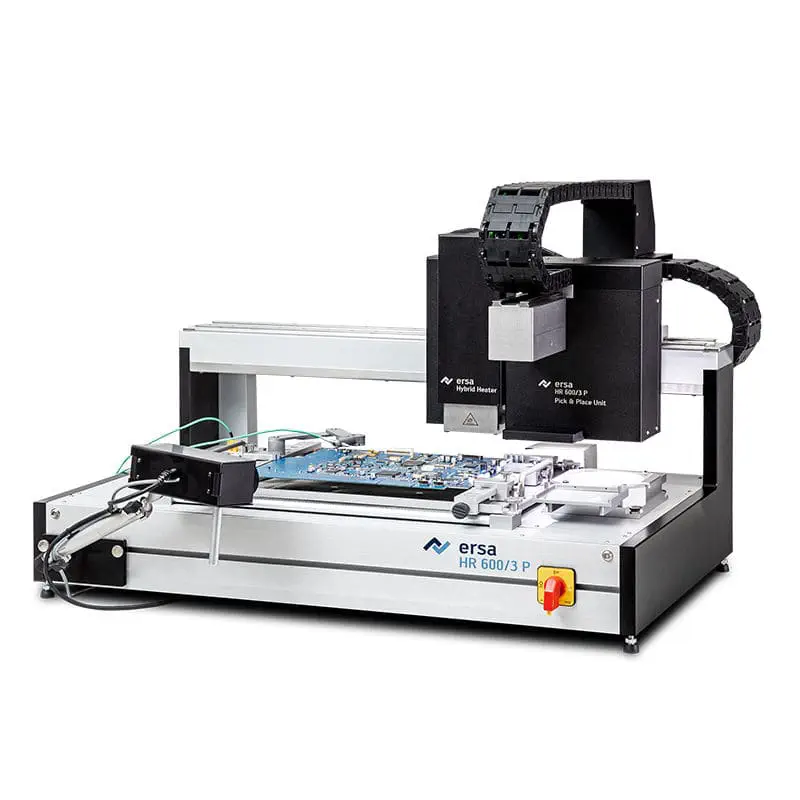
ERSA HR 600 XL – fixture terror.
ERSA HR 600 / 3P – fixture – terror.
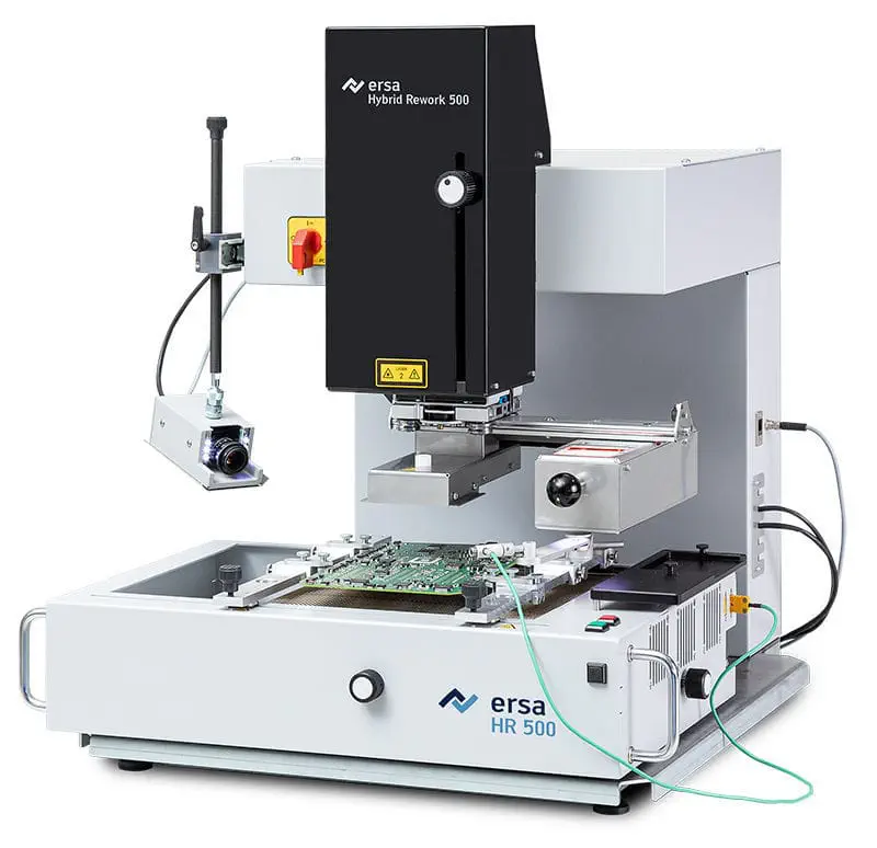
ERSA HR 500 – fixture – terror.
As accustomed us, ERSA it is on highest possible speed on his not alone aberrational competition track. Together with all inapt “professional manufacturers”, “well-known manufacturers”, “Chinese manufacturers”, “no-name manufacturers”, you name it what manufacturers. All that sell pizza machine, popcorn machine, Santa Claus cousin… have this worst approach to support a PCB / board for a rework process.
PCB support – worst practice – in general – click or touch or use menu to go.
As a professional in electronics sciences, as a professional in rework process, as you want a real Professional BGA Rework Station… you need… ELASTIC / FLEXIBLE method / solution / approach to support a PCB /board for a real professional BGA Rework process. Using a flexible / expandable but solid PCB support, you will give to PCB / board the possibility to expand / dilate when are heated and contract when are cooled.
PCB support – best practice – in general – click or touch or use menu to go.
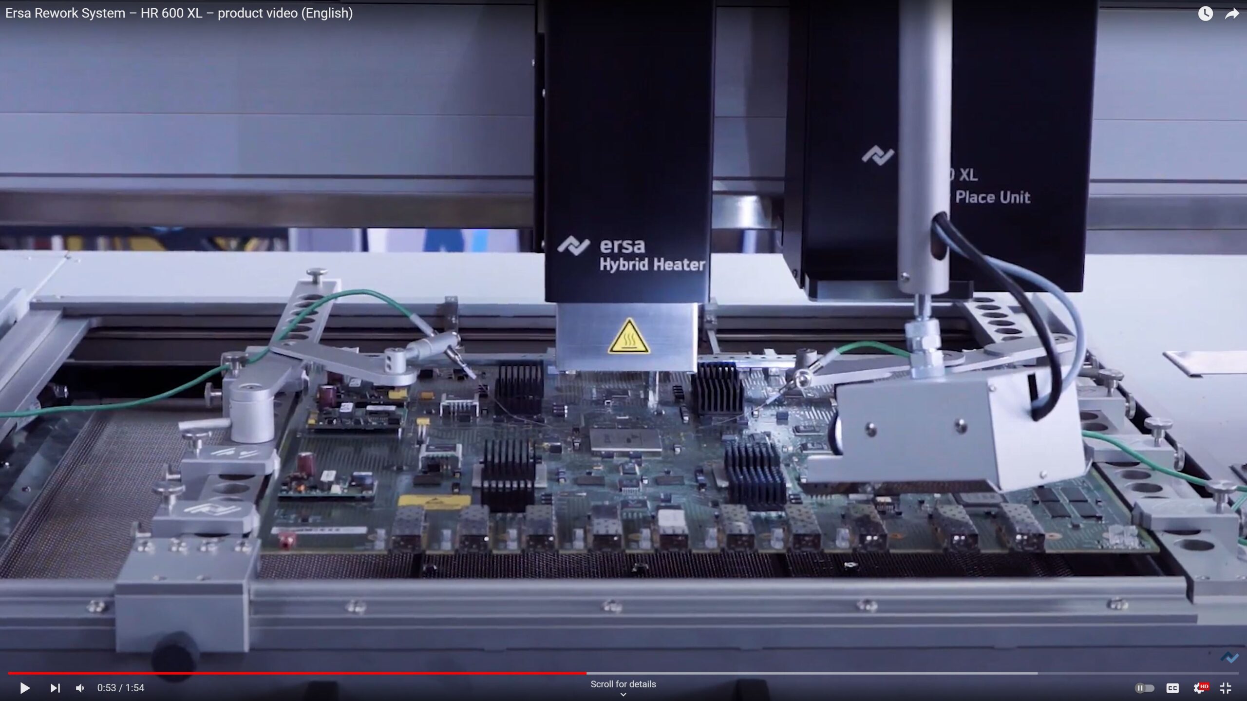
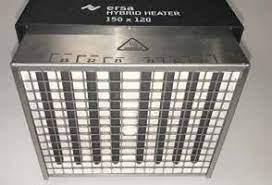
6 – Top heaters that ERSA use to heat a BGA / component are egual or more aberrational as all above. ERSA doen’t understand anything about rework process.
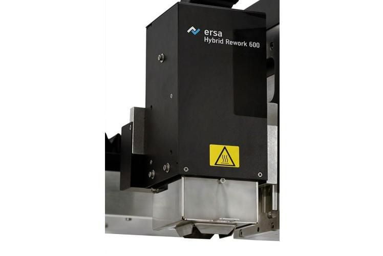
ERSA HR 600 – hybrid terror.
ERSA – top heater – terror.
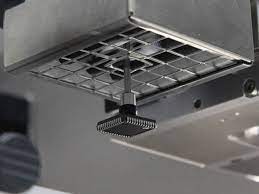
ERSA – another top heater – terror.
Straight to subject… ERSA use two of the worst methods in three possible ways (exist more ways…) to heat a BGA / chip. The first method is the hot air / nitrogen gas. The second method is “black IR” / medium infrared energy. And third method, the worst method is… hybridizing, (hybrid claiming) first two methods hot air / hot nitrogen + “Black-IR” / medium wave energy. With that wrong practice / bad practice / aberrational practice, they quit the possibility to control an inutile system.
The vertical position for their top heater are closest as possible to BGA / chip. They think… If it is a metallic top, BGA and the infrared energy can’t heat them (at that distance… Black-IR, medium wave energy, CAN heat the BGA / chip)… Well… they think that can’t heat… Well… put some hot air / nitrogen to be sure that BGA / chip are heated. These approaches make me lough. They are trying for a life to heat a BGA / chip / PCB / board… with heat – worst ever approach.
Top heater – worst practice – in general – click or touch or use menu to go.
I’ll speak in general… Trying to heat a BGA / chip with heating, it is a bad / wrong idea… A BGA / chip / PCB / board MUST be self heated. That mean that you would provide some magics energies to BGA / chip / PCB / board, and they’re self heating. On that manner, you will avoid the horrible heat that… heat all. This approach give you all world’s advantage and none disadvantage. That methods are the only one that respect all the best practice possibilities.
Top heater – best practice – in general – click or touch or use menu to go.
7 – P&P – placement method. Here, I don’t start with the words’ aberration, worst and so on. I don’t start with that only because ERSA was the first that try…
ERSA Pick and Place
ERSA Pick and Place
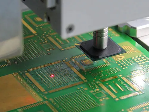
ERSA Pick and Place
… To implement that method / approach on a BGA Rework Station. The real problem that ERSA have… it’s that ERSA doesn’t have at least only one BGA Rework Station on his portfolio. ERSA have only pizza machines, popcorn machine, Santa Claus cousin on his portfolio. So the ERSA P&P problems start in another place. If we take a round on internet, we will find many P&P machines. Even the children’s on the internet have his own DIY… Pick and Place machines.
In fact, for BGA / Chips positioning on PCB / boards, the P&P (Pick and Place) systems are the best approach / best practice. But… ERSA doesn’t convince me.
If they have been succeeding in the Pick and Place functionality, they deserve congratulation, now came the difficult part for them… To find a Real Professional BGA Rework Station where implement that Pick and Place functionality as they until now it has only pizza machine, popcorn machines or Santa Claus cousin. If that over that past years have problems on his searching… you’ll don’t be worry… They have another many years in front of spend money (your money) in nothing.
They’re boring me, so… About process close view camera… same like all – wrong placed. The software are useless aberrant. The weight are stupid aberrant wrong and so on. If they don’t have a real professional BHA Rework Station… do not deserve loose time with this not important things.
Seems that ERSA have Awards. Or that fact ERSA claim. I wander… what an inutile / ignorant / energumens can give AWARDS for this garbage?!
Here you have my opinions about ERSA products from a scientifically / technologically / logically / electronically points of view. Take care about you’ll buy.